Recall the concept of density of states from Statistical Mechanics. By filling up the reciprocal space sphere of radius  and the dispersion relation
  , we can derive
![\[g_{\rm simple}(E) \ = \ \frac {m^{3/2}}{\hbar^3 \pi^2} \sqrt{2E}. \]](https://danielson13579.com/wp-content/ql-cache/quicklatex.com-21646731b5630c9ac5481b5ebb6ee2a3_l3.png "Rendered by QuickLaTeX.com")
This quadratic dependence of  for simple solids can be used to deduce the density of states of a semiconductor. Let
  denote the VBM, CBM of a semiconductor respectively. Below the VBM, the density of states (DOS) is determined by effective mass
  of the hole, and above CBM, by
  the effective mass of the electron. In symbols,
![\[g(E) \ = \ \begin{cases} \frac {m^{3/2}}{\hbar^3 \pi^2} \sqrt{2(E_V - E)} & E < E_V \\ 0 & E_V \leq E \leq E_C \\ \frac {m^{3/2}}{\hbar^3 \pi^2} \sqrt{2E} & E > E_C. \end{cases}\]](https://danielson13579.com/wp-content/ql-cache/quicklatex.com-51bf2ead57d6ab8b959a2632cf72f6e0_l3.png "Rendered by QuickLaTeX.com")
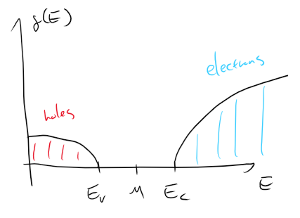
Figure. DOS plot of a simplified semiconductor.
The mean occupancy of a state is given by the Fermi-Dirac factor  . Here,
  is the chemical potential of the material and
![\[n_F(x) \ = \ \frac {1} {1 + e^x}. \]](https://danielson13579.com/wp-content/ql-cache/quicklatex.com-40cd6d1850d33898858af54be3d6ed95_l3.png "Rendered by QuickLaTeX.com")
We wish to derive the number of electrons and holes over a unit volume. This can be accomplished by integrating the product of mean occupancy times the density of states over all available energies.
![\[n \ = \ \int_{E_C}^\infty dE \ g(E) n_F(\beta(E-\mu)) \]](https://danielson13579.com/wp-content/ql-cache/quicklatex.com-651e278c8b22f7041010c41181e1919b_l3.png "Rendered by QuickLaTeX.com")
![\[p \ = \ \int_{-\infty}^{E_V} dE \ g(E) (1-n_F(\beta(E - \mu)))\]](https://danielson13579.com/wp-content/ql-cache/quicklatex.com-b9021a69bada537ff8bda0da5a8f8246_l3.png "Rendered by QuickLaTeX.com")
Holes are vacancies of electronic states, so the occupancy of a hole is the complement of mean electronic occupancy. The range of integration runs above CBM for the electrons, and under the VBM for holes. Upon algebra, these integrals simplify to the following.
![\[n \ = \ \left(\frac {m_e^* kT}{\pi}\right)^{3/2} \frac 1 {\sqrt 2 \hbar^3} e^{-\frac {E_C - \mu}{kT}}\]](https://danielson13579.com/wp-content/ql-cache/quicklatex.com-f6e5049384b2e0635ce51d7b2c35e21d_l3.png "Rendered by QuickLaTeX.com")
![\[p \ = \ \left(\frac {m_h^* kT}{\pi}\right)^{3/2} \frac 1 {\sqrt 2 \hbar^3} e^{\frac {E_V - \mu}{kT}}\]](https://danielson13579.com/wp-content/ql-cache/quicklatex.com-2abd07d4cf2b74a1d2add051031e25be_l3.png "Rendered by QuickLaTeX.com")
Multiplying the two charge carrier densities, notice that the chemical potential dependence  cancels out. By convention, write out the product as follows
![\[n p \ = \ n_i^2. \]](https://danielson13579.com/wp-content/ql-cache/quicklatex.com-44ec0898ca991bd146994e1ac8c2841f_l3.png "Rendered by QuickLaTeX.com")
The carrier density  is an intrinsic quantity of the semiconductor. An intrinsic semiconductor such as Silicon has
  . Since depends solely on temperature and effective masses of the carriers, adding charge carriers does not change the product. Thus, if electrons were to be added to the solid, the number of holes will decrease to preserve the product. Likewise, if vacancies were added, the number of electrons will decrease. Adding an impurity to the semiconductor can achieve this effect.
A n-type semiconductor is a type of a semiconductor with a donor impurity, meaning that the impurity carries more free electrons than the bulk. An example is Lead doped Silicon. Given that the charge density of the donor  is sufficiently high, attain
![\[n_o \ = \ N_d, \ \ p_o \ = \ n_i^2 / N_d. \]](https://danielson13579.com/wp-content/ql-cache/quicklatex.com-029f9f0b2557f171df65cb5b1c3dacf9_l3.png "Rendered by QuickLaTeX.com")
Typically,  for Silicon.
Likewise, a p-type semiconductor can be engineered by adding an acceptor impurity. In this case, the impurity has an additional vacancy in the valence band. An example is Boron doped Silicon. The carrier densities are determined by the acceptor density  by the formula
![\[n_o \ = \ n_i^2/N_a, \ \ p_o \ = \ N_a. \]](https://danielson13579.com/wp-content/ql-cache/quicklatex.com-ddce0da3865b9cc2bb41d727c3d795a4_l3.png "Rendered by QuickLaTeX.com")
Likewise,  for Silicon.
The charge density increases exponentially with respect to  in low temperatures. Suppose that the chemical potential is known (one approximation is to claim
  ). Then, the slope of the plot of log electron density verses inverse temperature is
  . Repeating this procedure for the log hole density plot, we can obtain the quantity
  and
and  . Add the two quantities to derive the band gap.
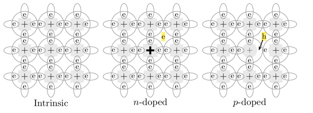
Figure. Demonstrative diagram of n-doped and p-doped semiconductor. The donor impurity of the n-doped semiconductor adds a free electron to the solid as the acceptor impurity incurs a vacancy in a p-doped semiconductor.
We have derived the number density of electrons and hole of a semiconductor and deduced that the product of the two is invariant. This invariance can be used to engineer the semiconductor through doping.
References
The Oxford Solid State Basics – Paperback – Steven H. Simon – Oxford University Press
Leave a Reply