A solid is characterized by a periodic arrangement of atoms. This periodic arrangement allows us to characterize a solid as arrangement of atoms along repeated instances of a unit cell. A single atom in a unit cell is repeatedly arranged over entire space, and this arrangement is called a lattice. To understand optical properties of the lattice, physicists study the reciprocal space. Each wavevector  is represented vector in the reciprocal lattice, and it is possible to associate an energy using Fourier Transforms.
A path along the Wigner-Seitz cell effectively captures the energy of different wavevectors in reciprocal space. This path is called a k-path; a k-path passes through high-symmetry points, which allows us to deduce energies in reciprocal space using crystal symmetries.
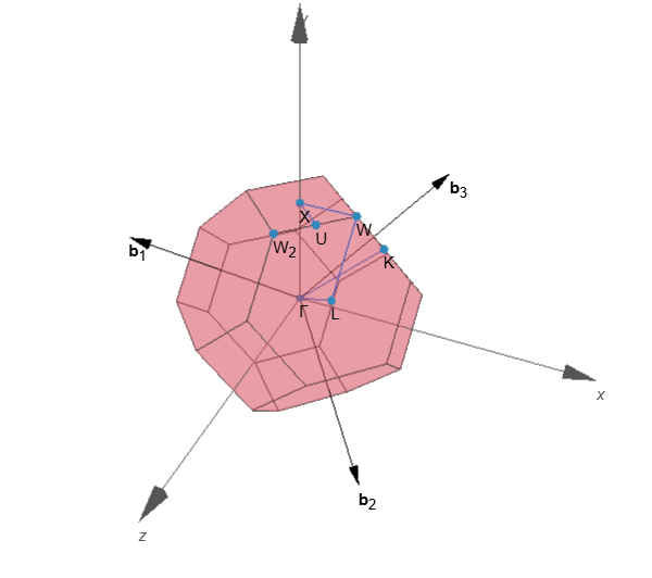
Figure. Wigner-Seitz cell and a k-path of NbN. The path begins from the  point located at the center of a cell, reaches the cell boundary through the hexagonal face. Then, the path iterates over the high symmetry points at the edges of the cell. The path ends at point X, the center of the square face.
The energy band plot has three major features. The first is the Fermi energy which is the energy level of an electron at zero temperature. Conventionally, energy bands notate  and plot
  instead of raw value of energy. A band that lives above the Fermi energy is called a conduction band, and the one that lives below is called a valence band.
The electrical property of a solid is determined by the energy gap,  . It is defined by the difference between Conduction Band Minimum (CBM) and the Valence Band Maximum (VBM). Insulators have large energy gaps while semiconductors have small energy gaps. If the gap energy is negative, the resulting solid is a conductor.
Most charged particles of a solid is nearly fixed in space. Electrons in the valence band and the protons in the nucleus are examples. Thus, to understand the movement of charge in a solid, we study charge carriers. Electrons in the conduction band is a charge carrier. In some solids, a vacancy in the conduction band can act like a charge carrier. Though these vacancies are not particles, we denote them as holes, which act as positive charge carriers.
Apart from the formal mass of these charge carriers, we define an effective mass used for calculations. Approximate the curvature of the conduction band around the local minimum using a quadratic function. Dividing by  appropriately gives the following formula.
![\[\frac 1 {m^*_{e}} \ = \ \frac 1 {\hbar^2} \frac {\partial^2}{\partial k^2} E(k)\]](https://danielson13579.com/wp-content/ql-cache/quicklatex.com-8e85adce58542c082dbc5adbb5475823_l3.png "Rendered by QuickLaTeX.com")
Higher curvature of the band means that the periodic potential has a strong effect on carrier movement, thus the effective mass is low. On the other hand, if the curvature is small, the effect of periodic potential on particle movement is small and the particle has a high effective mass.
The effective mass of an electron need not be positive. Depending on the region of the band, the effective mass can be negative. However, the effective mass of a hole is fixed to be positive by convention.
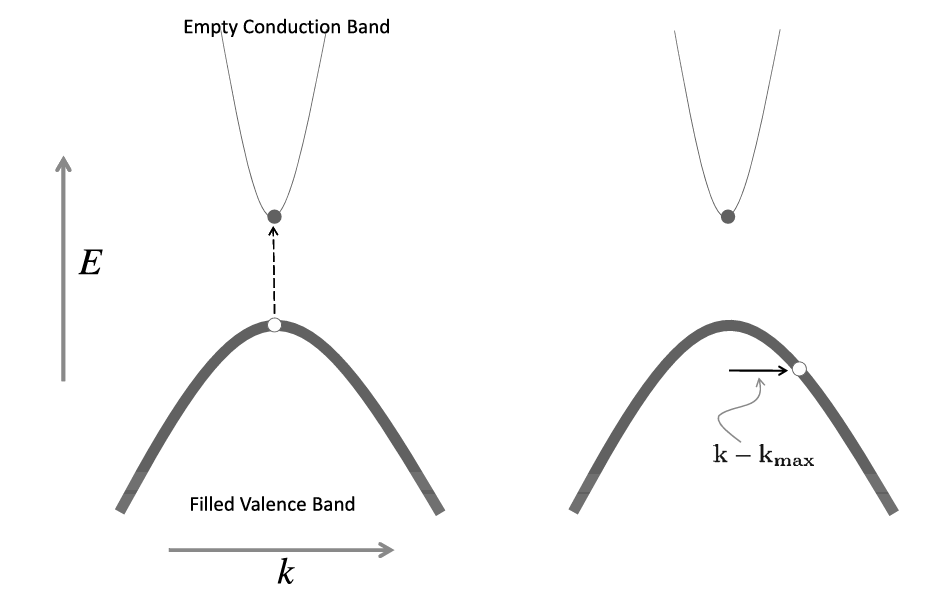
Figure. Holes and electrons on a simplified parabolic band. (Oxford Solid State Basics)
Typically, electrons live at the bottom of the conduction band that resembles a convex quadratic. Holes live at the top of a concave quadratic. It seems counterintuitive that the charge carrier occupies the maximum energy among all allowable states. However, the hole is imaginary, and the real charge carriers which are the electrons occupy the lowest energy states.
The momentum of an electron can be computed from crystal momentum, i.e.  . The momentum of a hole incurs an additional negative sign, i.e.
  . A filled band has zero momentum, and removing an electron at the position of the hole gives a desired hole configuration. Thus, the momentum of the hole is negative of that of an electron.
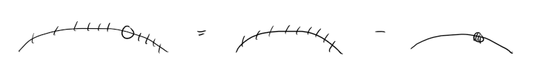
Figure. Demonstrative diagram of a single hole arrangement. Removing a single electron from a completely filled band yields a hole arrangement.
References:
The Oxford Solid State Basics – Paperback – Steven H. Simon – Oxford University Press
16. Band Structure and Optical Properties of Solids | University of Oxford Podcasts
Leave a Reply